
Synopsys Cloud
Cloud native EDA tools & pre-optimized hardware platforms
Request a Free Trial →
A wide variety of photonic devices compatible with silicon processing have been developed. These include both passive and active devices such as waveguides, modulators, and detectors. The missing component is a light source. This is due to the fact that silicon is an indirect gap material. To resolve this limitation, much effort has been spent on integrating direct gap materials onto silicon substrates. The process of wafer bonding has provided this capability.
Structurally, active III-V layers are bonded on top of waveguiding layers in a silicon on insulator system (SOI). These active layers must be close enough to the silicon waveguide so that a sufficient overlap exists between them and the waveguide mode to achieve lasing. A schematic of such a layer structure is shown in Figure 1. In the example presented here, a ridge waveguide is etched into the silicon layer (0.69µm thick) on top of the buried oxide (BOX). The ridge width is 2.5µm and the etch depth is 0.52µm. The III-V region contains 8 AlGaInAs Quantum Well / Barrier layers as well as cladding and electron blocking layers. The composition of the active layers was designed for 1310nm operation. Such structures have also been realized for 1550 nm [1]. Implantation was used to restrict current in the active layers. The width used for this current confinement was 5mm and the length of the active region was 860µm.
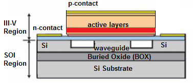
Figure 1. SEL structure showing a III-V material system bonded on top of SOI layers.
Figure 2 shows the fundamental and second order transverse modes. The confinement factors are, respectively, ~1% and ~8%. However, these can be different in the fabricated device due to variations in the as-grown refractive indexes. It can be seen from the mode profiles that the higher order mode has the larger confinement factor, and will therefore have the lower threshold. Lastly, it should be noted that the current confinement can greatly impact the lasing threshold as well, by increasing the carrier overlap with the optical mode.

Figure 2. Fundamental mode (left) and second order transverse mode (right) for the structure of Figure 1.
The lasing performance of this device is shown in Figure 3, where the simulated L-I curve is for 15°C and is shown as a dashed line, while the measure L-I results for several temperatures are shown as solid lines. As stated above, this power is in the 2nd order transverse mode. Finally, both simulated and measured results show the power that is coupled from a single facet of the device into an optical fiber. The measured coupling loss into the fiber is estimated to be around 4.6dB [1].
![Figure 3. Simulated result at 15°C (dashed line) and measured results [1] (solid lines) for output power (due to 2nd order transverse mode) coupled from one facet into a fiber | Synopsys](/photonic-solutions/product-applications/lasers/hybrid-silicon-laser/_jcr_content/root/synopsyscontainer/column/colLeft/column_68510958_copy/colLeft/image.coreimg.gif/1596144745937/0717july-results.gif)
Figure 3. Simulated result at 15°C (dashed line) and measured results [1] (solid lines) for output power (due to 2nd order transverse mode) coupled from one facet into a fiber.
For more information, please contact photonics_support@synopsys.com.
References
1. Hsu-Hao Chang, Alexander W. Fang, Matthew N. Sysak, Hyundai Park, Richard Jones, Oded Cohen, Omri Raday, Mario J. Paniccia, and John E. Bowers, “1310nm silicon evanescent laser,” Optics Express, Vol. 15, No. 18, pp. 11466-71, September 2007.


