


The AI and HPC industries are advancing toward chiplet-based designs to achieve superior performance, as traditional monolithic SoCs face scaling challenges. Heterogeneous integration is driving semiconductor innovation but adds complexity to chip design, requiring advanced testing methodologies and improved Automated Test Equipment (ATE). Increasing test patterns and limited package pins demand high-bandwidth IOs, while advancements in ATE capabilities further necessitate optimized GPIOs to support higher-speed, efficient and low-cost testing.
Synopsys High-Speed Test IO IP is a cutting-edge IO interface solution that enables efficient, high-speed testing of complex semiconductor designs while minimizing hardware complexity and cost. It achieves this by supporting high data rates (up to 2.5Gbps) for testing, reusing limited package pins for multiple modes (serving as test ports during manufacturing, enabling high-speed clock observation during debugging, and functioning as GPIO during production), and eliminating the need for complex protocols or calibration sequences. This simplifies testing, reduces development time and costs, and ensures high test coverage and reliability for advanced AI, HPC, and chiplet-based designs.
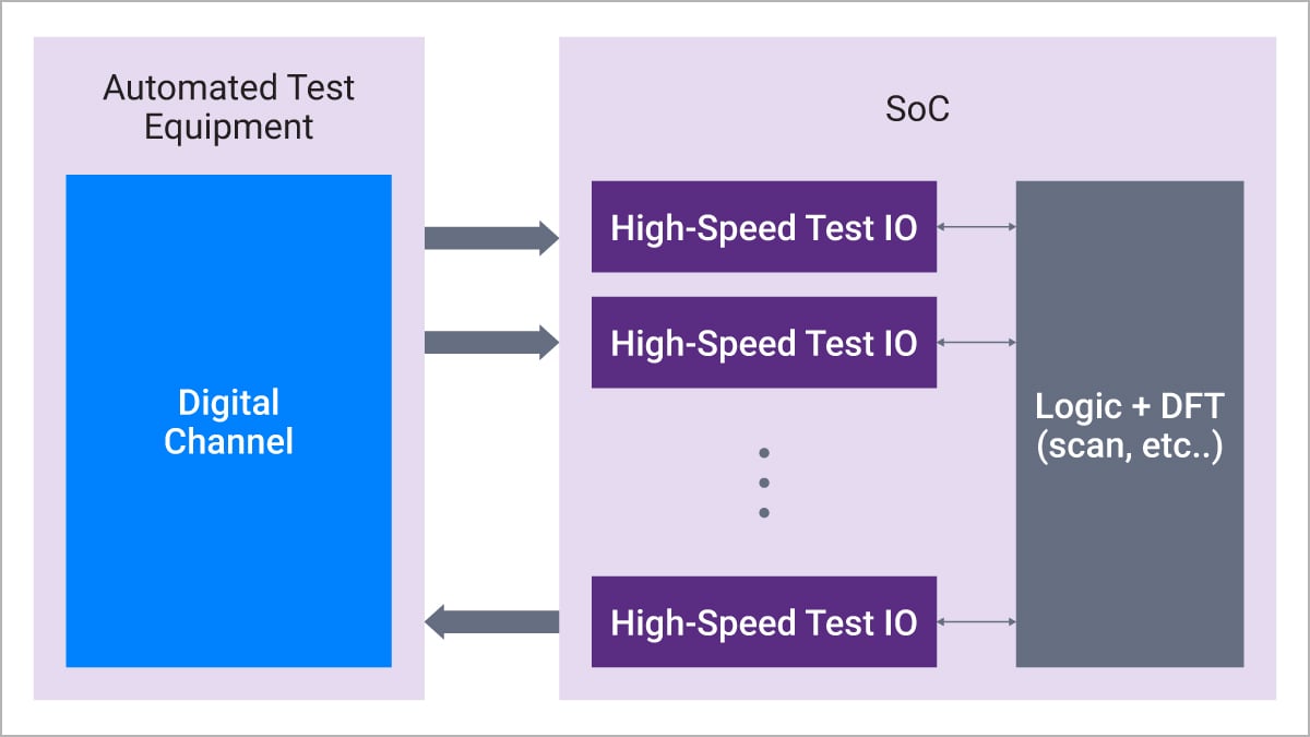
Synopsys High-Speed Test IO Block Diagram
Highlights
Product Details


Find Your IP
Search for IP
Quickly identify and access the right IP solutions for your project needs.
Foundation IP Selector
Find embedded memory and logic IP for your SoC design.
Non-Volatile Memory IP Selector
Find silicon-proven NVM IP for your SoC design needs.