


Synopsys IP Technical Bulletin Article
Building a Bridge from PCI Express to AMBA 3 AXI On-Chip Bus
PCI Express® was developed as the next generation interface to replace PCI®, PCI-X®, and AGP for computer expansion cards and graphics cards. It provides better bandwidth performance and the lower manufacturing costs, has layered architecture, and is backward compatible to the previous PCI software infrastructure and easy to use. AMBA is an industry standard which drives the high performance, enable high reusability and high connectivity. The Synopsys DesignWare PCI Express IP solution provides an AXI Bridging capability for directly adding a PCI Express link to an AXI system fabric. This can significantly reduce the time to design PCI Express into an AXI-based SOC. In this paper, we will discuss the process of building a bridge from PCI Express to the industry-standard AMBA® 3 AXI™ on-chip bus.PCI Express Architecture Basics
PCI Express is a serial, point-to-point interface. It comprises of four device types:- The Root Complex initializes the PCI Express fabric and is usually tied to the microprocessor.
- The Switch routes data between multiple PCI Express ports.
- The Endpoint is the requestor or completer of PCI Express transactions and is in the end application. Generally, you will have more endpoints in your design than any other type.
- Finally, the bridge is just what the name implies. It bridges between PCI Express and other interfaces; like PCI.
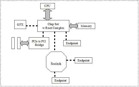
Figure 1. PCI Express Topology
- Mechanical, which define things like the connectors
- The Physical Layer. The Physical layer is broken into two portions, the logical layer and the electrical layer. There is also a specification available called the Physical Interface for PCI Express or “PIPE” that defines the interface between the PHY and the rest of the physical interface.
- The Data Link Layer
- The Transaction Layer
- And the Application Layer
AMBA Based Sub-system Basics
AMBA based sub-system typically consists of a high performance system interconnect bus. The typical components in AMBA sub-system are very similar to PCI system except a component called DMA. DMA stands for direct memory access. AMBA system has a centralized DMA unit which can perform data movement between memories and IO devices. PCI system has DMA resides in most of the IO devices.
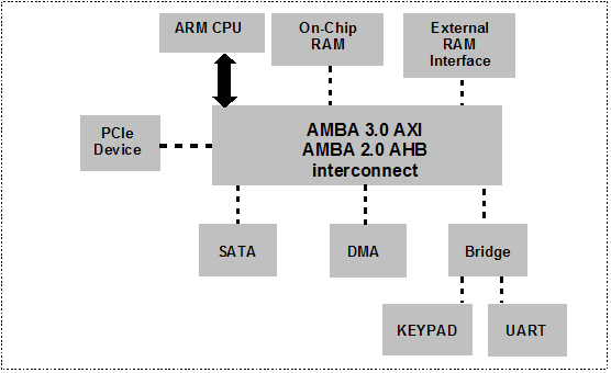
Figure 2: AMBA Sub-system Toplogy
Synopsys Solution for PCI Express to AXI Bridge
Synopsys offers a complete PCI Express solution including digital cores, PHY IP and verification IP. The digital cores are configurable and scalable to meet multiple application requirements and have user-friendly native application interfaces or AHB/AXI interface.
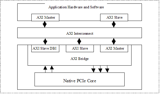
Figure 3: System Level View of the DWC PCIe AXI Core
PCI Express to AXI Bridge Architecture
The PCI Express to AXI Bridge provides an interface between the DesignWare PCI Express IP's native application interface and the AXI interconnect. It enables a remote PCIe device to be either an AXI slave or an AXI master. The bridge contains AXI master and slave protocol handlers, internal slave and master control for generic request and response interfaces, a packet composer, and a packet decomposer for response formation. The slave and master protocol handlers support the AXI protocol conversion between an AXI transfer and a generic transfer within the bridge. The slave and master generic interface supports the conversion of an AXI transfer to a PCIe transaction. The packet composer and decomposer support the segmentation and reassembly of a PCIe transaction.
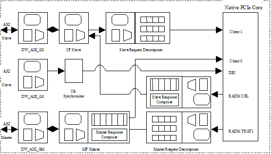
Figure 4: AXI Bridge Architecture
Summary
It's pretty complex to develop a bridge to PCI Express from your Syetem-on-Chip design. This requires a fair amount of knowledge of the PCI Express standard, and the design can be tough. Using DesignWare PCI Express with AXI Interface IP makes your design task considerably easier. The DesignWare PCI Express IP is configurable, scalable, synthesizable, and is easily to be added into SoC designs.Search Tools