


Synopsys IP Technical Bulletin Article

DesignWare Mobile Storage Host Controller Core: Handling Timing Requirement for SD3.0 Cards
This article describes the timing requirement needed for interfacing the DesignWare Mobile Storage (DWC_mobile_storage) Host Controller core (version 2.20a and version 2.30a) to SD cards that have different modes of operation. It explains how an external clock multiplexor structure is needed to meet the timing requirements across the various card operating modes described in the SD Memory card specification Version 3.0.P.K. Venkataraghavan
Vishwanath Kakarla
Venkata Giri Kumar P
Devashish Dutta
Phase shift values must be determined after place and route and then used for back annotation. This article describes the structure with typical delays at a 65nm process technology. The I/O pad delays should be kept to a minimum in order to reduce stress on timing at both the host controller and card interface.
| MODE | Maximum Freq of Operation | Hold Time Requirement | Setup Time Requirement |
|---|---|---|---|
| SDR104 | 200Mhz | .8ns | 1.4ns |
| SDR50 | 100Mhz | .8ns | 3ns |
| DDR50(CMD line) | 50Mhz | .8ns | 6ns |
| DDR50(DAT line) | 50Mhz | .8ns | 3ns |
| SDR25 | 50Mhz | 2ns | 6ns |
| SDR12 | 25Mhz | 5ns | 5ns |
| Identification Mode | 400Khz | 5ns | 5ns |
| Table-1: SD 3.0 specification for card input timings | |||
Table 2 below shows the card output timing requirements that act as constraints for the Mobile Storage Host Controller input path from the card.
| MODE | Maximum Freq of Operation | Maximum Card Output Delay |
|---|---|---|
| SDR104 | 200Mhz | 10 |
| SDR50 | 100Mhz | 7.5 |
| DDR50(CMD) | 50Mhz | 13.7 |
| DDR50(DAT) | 50Mhz | 7 |
| SDR25 | 50Mhz | 14 |
| SDR12 | 25Mhz | 14 |
| Identification Mode | 400Khz | 50 |
| Table-2: Card output delay timing requirements | ||
To use the SDR104 mode, the user must select the FIFO size based on the number of blocks to be used. If one block of data is to be read or written, then the FIFO size should be at least 512 bytes. If four blocks (512 bytes * 4) are to be used, then the user must select a FIFO depth of at least 2K bytes while configuring the DWC_mobile_storage host controller. In these circumstances, for the SDR104 mode, the maximum number of blocks that can be programmed in one transfer are:
- 64 when the AHB data width is selected as 64
- 32 when the AHB data width is selected as 32
The following RTL configuration requirements and programming flow for software drivers should be used in order to use the DWC_mobile_storage host controller in SDR104 mode applications:
- FIFO size should be selected as multiple of 512 bytes at time of RTL configuration.
- Program BYTCNT register to value equal to multiple of 512 bytes and less than or equal to FIFO size.
- Program BLKSIZ register to 512-block length fixed to 512 in SDR104 mode.
- If transfer size is more than FIFO size, then it should be split into multiple transfers-size of each transfer can be equal to FIFO size; a new transfer is programmed after data done is received for previous transfer.
The DWC_mobile_storage host controller uses the following clocks to achieve a reliable communication with the interfaced cards:
- cclk_in - Clock the logic in the Card Interface Unit (CIU) clock domain.
- cclk_in_drv - Has the same frequency as cclk_in, but is phase shifted. Satisfies the minimum hold time requirement of 5 ns at the input to the cards while operating in SDR12 or identification modes.
- cclk_in_sample - Has the same frequency as cclk_in, but is phase shifted. Provides a "best sampling window" for the DWC_mobile_storage host controller while reading data from the card. Has the same frequency as cclk_in, but is phase shifted. The need for cclk_in_drv is to satisfy a minimum hold time requirement of 5ns at the input to the cards while operating in the SDR12 or Identification modes.
The following are recommendations for clock generation:
- The cclk_in frequency input to the DWC_mobile_storage core can be switched, depending on the data rate. For example, if the interfaced card is communicating in the SDR50 mode, then cclk_in = 50 Mhz; if the interfaced card is communicating in the SDR104 mode, then cclk_in = 200 Mhz.
- You should ensure that there are no glitches in the clock inputs while switching clock frequencies. The cclk_in_drv and cclk_in _sampkle_clock frequrencies mnyst switch in relation to cclk_in frequencies.
- The cclk_in_drv and cclk_in_sample clocks are phase-shifted versions of cclk_in. The value of the phase shift should be selectable, based on the enumerated data rate. The phase shift can have a resolution of 90 degrees with respect to the cclk_in clock period.
The following assumptions pertain to the timing and clocking recommendations:
- The DWC_mobile_storage host controller in the design is instantiated with one port.
- The following delays are assumed:
- Host-controller output path:
- Delay_O = cclk_in to cclk_out delay = 1.4ns (Typical value)
- Host-controller input path:
- tODLY = cclk_out to cdata_in delay = max value (specified in Table 2)
- Delay_I = IO_pad delay + routing delays within host controller = 2.35 ns (typical value)
- Delay_S = Delay_O + Delay_I = 3.75 ns
- Delay(total turnaround) between Host Controller output and input = tODLY + Delay_S (Delay_O + Delay_I)
- Host-controller output path:
- Synthesis is done in 65nm; setup and hold times for the flip-flops within the DWC_mobile_storage host controller are assumed to be 1 ns.
- Figure 1 below illustrates how the DWC_mobile_storage host controller and card delays relate to each other:
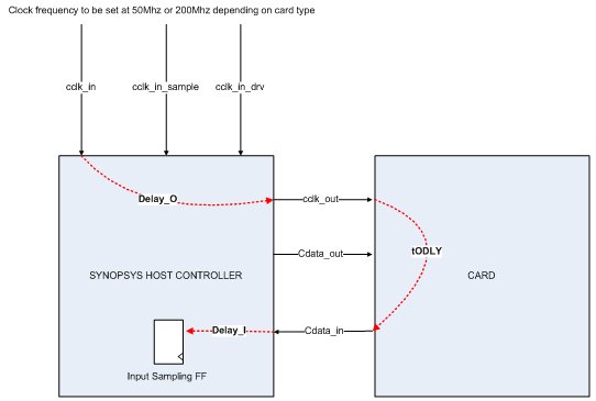
Figure 1 Clock frequency set at 50 MHz or 200 MHz, depending on card type
| MODE | Freq of Operation | Input Frequency (cclk_in) | D i v i d e r |
Hold time delays to be introduced (clk_in_drv) through phase shifters |
Hold time delays to be checked |
Resultant Hold Time |
Setup time to be checked |
Resultant Setup Time |
Final Effective Result | Comments |
|---|---|---|---|---|---|---|---|---|---|---|
| SDR104 | 200Mhz | 200Mhz | 1 | 1.25ns | .8ns | 4.85 | 1.4ns | 0.15 | Fail | |
| 2.5ns | 1.1 | 3.9 | Pass | |||||||
| 3.75ns | 2.35 | 2.65 | Pass | This is suggested to keep the resultant hold time to be away from 1ns | ||||||
| SDR50 | 100Mhz | 200Mhz | 2 | 1.25ns | .8ns | 9.85 | 3ns | 0.15 | Fail | |
| 2.5ns | 1.1 | 8.9 | Pass | |||||||
| 3.75ns | 2.35 | 7.65 | Pass | This is suggested to keep the resultant hold time to be away from 1ns | ||||||
| DDR50 (CMD line) |
50Mhz | 50Mhz | 1 | 5ns | .8ns | 3.6 | 6ns | 16.4 | Pass | This is suggested to keep it same as DAT line |
| 10ns | 8.6 | 11.4 | Pass | |||||||
| 15ns | 13.6 | 6.4 | Pass | |||||||
| DDR50 (DAT line) |
50Mhz | 50Mhz | 1 | 5ns | .8ns | 3.6 | 3ns | 6.4 | Pass | Only 90 degree phase shift could match both setup and hold time |
| 10ns | 8.6 | 1.4 | Fail | |||||||
| 15ns | 3.6 | 6.4 | Fail | Start bit for half cycle | ||||||
| SDR25 | 50Mhz | 50Mhz | 1 | 5ns | 2ns | 3.6 | 6ns | 16.4 | Pass | |
| 10ns | 8.6 | 11.4 | Pass | Has better margin for both setup and hold time. | ||||||
| 15ns | 13.6 | 6.4 | Pass | |||||||
| SDR12 | 25Mhz | 50Mhz | 2 | 5ns | 5ns | 3.6 | 5ns | 36.4 | Fail | |
| 10ns | 8.6 | 31.4 | Pass | |||||||
| 15ns | 13.6 | 26.4 | Pass | Has better margin for both setup and hold time. | ||||||
| Identification Mode | 400Khz | 50Mhz | 125 | 5ns | 5ns | 3.6 | 5ns | 2516.4 | Fail | |
| 10ns | 8.6 | 2511.4 | Pass | |||||||
| 15ns | 13.6 | 2506.4 | Pass | Has better margin for hold time. Setup time is anyways very large. | ||||||
| Table-3: Simulation-based test results for Host controller output path | ||||||||||
Light Green Pass: Hold tome or Setup time pass independently, does not guarantee both
Red: Margins below 1ns
| MODE | Freq of Operation | Input Frequency (cclk_in) | Divider ratio | Sampling delays to be introduced, by phase shifter | Delays on cdata_in (introduced by card) | Sampling Result, data integrity checks | available hold time | available setup time | Final Result (combines data integrity, setup/hold time > 1ns, startbit validity) | Comment |
|---|---|---|---|---|---|---|---|---|---|---|
| SDR104 | 200Mhz | 200Mhz | 1 | 0ns | 0ns | Pass | 3.75 | 1.25 | Pass | |
| 4.8ns | Pass | 3.55 | 1.45 | |||||||
| 5ns | Pass | 3.75 | 1.25 | |||||||
| 9.6ns | Pass | 3.35 | 1.65 | |||||||
| 10ns | Pass | 3.75 | 1.25 | |||||||
| 1.25ns | 0ns | Pass | 2.5 | 2.5 | Pass | |||||
| 4.8ns | Pass | 2.3 | 2.7 | |||||||
| 5ns | Pass | 2.5 | 2.5 | |||||||
| 9.6ns | Pass | 2.1 | 2.9 | |||||||
| 10ns | Pass | 2.5 | 2.5 | |||||||
| 2.5ns | 0ns | Pass | 1.25 | 3.75 | Fail | |||||
| 4.8ns | Pass | 1.05 | 3.95 | |||||||
| 5ns | Pass | 1.25 | 3.75 | |||||||
| 9.6ns | Pass | 0.85 | 4.15 | |||||||
| 10ns | Pass | 1.25 | 3.75 | |||||||
| 3.75ns | 0ns | Pass | 0 | 5 | Fail | |||||
| 4.8ns | Pass | 4.8 | 0.2 | |||||||
| 5ns | hangs | |||||||||
| 9.8ns | Pass | 4.6 | 0.4 | |||||||
| 10ns | hangs | |||||||||
| SDR50 | 100Mhz | 200Mhz | 2 | 0ns | 0ns | Pass | 3.75 | 6.25 | Pass | |
| 3.6ns | Pass | 7.35 | 2.65 | |||||||
| 7.5ns | Pass | 1.25 | 8.75 | |||||||
| 1.25ns | 0ns | Pass | 2.5 | 7.5 | Fail | |||||
| 3.6ns | Pass | 6.1 | 3.9 | |||||||
| 7.5ns | Pass | 9.85 | 0.15 | |||||||
| 2.5ns | 0ns | Pass | 1.25 | 8.75 | Pass | |||||
| 3.6ns | Pass | 4.85 | 5.15 | |||||||
| 7.5ns | Pass | 8.75 | 1.25 | |||||||
| 3.75ns | 0ns | Pass | 5 | 5 | Pass | |||||
| 3.6ns | Pass | 8.6 | 1.4 | |||||||
| 7.5ns | Pass | 2.5 | 7.5 | |||||||
| DDR50(DAT) | 50Mhz | 50Mhz | 1 | 0ns | 0ns | Pass | 3.75 | 6.25 | Fail | All the test are failures as the total delay is more than 10ns; 1.4ns + 7ns + 2.35 ns = 10.75ns which is greater than the allowed delay of 10ns |
| 3.5ns | Pass | 7.25 | 2.75 | |||||||
| 7ns | Fail | 0.75 | 9.25 | |||||||
| 5ns | 0ns | Fail | 8.75 | 1.25 | Fail | |||||
| 3.5ns | Pass | 2.25 | 7.75 | |||||||
| 7ns | Pass | 6.4 | 3.6 | |||||||
| 10ns | 0ns | Fail | 3.75 | 6.25 | Fail | |||||
| 3.5ns | Fail | 7.25 | 2.75 | |||||||
| 7ns | hangs | |||||||||
| 15ns | 0ns | hangs | Fail | |||||||
| 3.5ns | Fail | 2.25 | 7.75 | |||||||
| 7ns | Fail | 5.75 | 4.25 | |||||||
| SDR25, DDR50(CMD) | 50Mhz | 50Mhz | 1 | 0ns | 0ns | Pass | 3.75 | 16.25 | Pass | |
| 7ns | Pass | 10.75 | 9.25 | |||||||
| 14ns | Pass | 17.75 | 2.25 | |||||||
| 5ns | 0ns | Pass | 18.75 | 1.25 | Pass | |||||
| 7ns | Pass | 5.75 | 14.25 | |||||||
| 14ns | Pass | 12.75 | 7.25 | |||||||
| 10ns | 0ns | Pass | 13.75 | 6.25 | Fail | |||||
| 7ns | Pass | 0.75 | 19.25 | |||||||
| 14ns | Pass | 7.75 | 12.25 | |||||||
| 15ns | 0ns | Pass | 8.75 | 11.25 | Pass | |||||
| 7ns | Pass | 15.75 | 4.25 | |||||||
| 14ns | Pass | 2.75 | 17.25 | |||||||
| SDR12 | 25Mhz | 50Mhz | 2 | 0ns | 0ns | Pass | 3.75 | 36.25 | Pass | |
| 7ns | Pass | 10.75 | 29.25 | |||||||
| 14ns | Pass | 17.75 | 22.25 | |||||||
| 5ns | 0ns | Pass | 38.75 | 1.25 | Pass | |||||
| 7ns | Pass | 5.75 | 34.25 | |||||||
| 14ns | Pass | 12.75 | 27.25 | |||||||
| 10ns | 0ns | Pass | 33.75 | 6.25 | Fail | |||||
| 7ns | Pass | 0.75 | 39.25 | |||||||
| 14ns | Pass | 7.75 | 32.25 | |||||||
| 15ns | 0ns | Pass | 8.75 | 31.25 | Pass | |||||
| 7ns | Pass | 15.75 | 24.25 | |||||||
| 14ns | Pass | 22.75 | 17.25 | |||||||
| Identification Mode | 400Khz | 50Mhz | 125 | 0ns | 0ns | Pass | 3.75 | 2516.3 | Pass | |
| 25ns | Pass | 28.75 | 2491.3 | |||||||
| 50ns | Pass | 53.75 | 2466.3 | |||||||
| 5ns | 0ns | Pass | 2518.8 | 1.25 | Pass | |||||
| 25ns | Pass | 23.75 | 2496.3 | |||||||
| 50ns | Pass | 48.75 | 2471.3 | |||||||
| 10ns | 0ns | Pass | 2513.8 | 6.25 | Pass | |||||
| 25ns | Pass | 28.75 | 2491.3 | |||||||
| 50ns | Pass | 43.75 | 2476.3 | |||||||
| 15ns | 0ns | Pass | 8.75 | 2511.3 | Pass | |||||
| 25ns | Pass | 33.75 | 2486.3 | |||||||
| 50ns | Pass | 58.75 | 2461.3 | |||||||
| Table 4: Simulation test results for input path | ||||||||||
Orange: Margins below 2ns, but not as good as margins marked in green.
Red: Margins below 1ns The timing in the DDR50 (DAT) fails because the total delay is greater than 10ns. This is calculated as TODLY max + Delay_S = 7 + 2.35 + 1.4 = 10.75ns. The following can meet the DDR50 (DAT) timing requirements:
- The delay on the cdata_in from the card has a delay greater than .75ns, where the cclk_in_sample has a 90 degree (5ns) phase shift.
- Within DWC_mobile_storage_ciu, delay the cclk_in to other modules by 1.4ns except for DWC_mobile_storage_clkcntl.v. This eliminates phase shifts on cclk_out and the cclk_in
- "Physical Layer Specification", Part 1, Version 3.01, Draft 0.82