


Synopsys IP Technical Bulletin Article
How to Connect Your DesignWare USB 2.0 nanoPHY to Your DesignWare USB 2.0 OTG Controller
This application note describes the connectivity and power-on reset sequence between the Synopsys DesignWare USB 2.0 nanoPHY and the DesignWare USB 2.0 Hi-Speed (HS) On-The-Go (OTG) Controller Subsystem. 1. Supported Speed ModesBy Doug Aida, Technical Writer
The DesignWare USB 2.0 nanoPHY and USB 2.0 HS OTG Subsystem support all the speed modes required by the USB 2.0 specification. Together, they support high speed, full speed, and low speed in Host mode and high speed and full speed in Device mode. 2. Interfacing the DesignWare USB 2.0 nanoPHY With the DesignWare USB 2.0 HS OTG Subsystem
This section describes the connectivity that applies when the USB 2.0 HS OTG Subsystem is configured to use the UTMI+ interface. If the USB 2.0 HS OTG Subsystem is configured to support the UTMI+ (Level 3, non-OTG) specification, see Section 2.1, below titled, USB 2.0 HS OTG Subsystem Configured to Support the UTMI+ (Level 3, Non-OTG) Specification. When the USB 2.0 HS OTG Subsystem is configured as a non-HNP-, non-SRP-capable OTG controller, the associated application can operate as a non-OTG host or device. If the USB 2.0 HS OTG Subsystem is configured to support the UTMI+ (Level 3, OTG) specification, see Section 2.2, of this application note, titled, USB 2.0 HS OTG Subsystem Configured to Support the UTMI+ (Level 3, OTG) Specification. Only signals that are relevant to the UTMI/UTMI+ specification or that require special consideration are shown. For information about these signals, refer to the signal descriptions in each product's databook. 2.1. USB 2.0 HS OTG Subsystem Configured to Support the UTMI+ (Level 3, Non-OTG) Specification
Figure 1 shows a high-level block diagram of the USB 2.0 nanoPHY and USB 2.0 HS OTG Subsystem when configured to support the UTMI+ (Level, 3, non-OTG) specification.
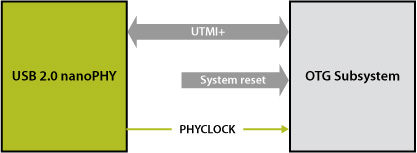
Figure 1. USB 2.0 nanoPHY and USB 2.0 HS OTG Subsystem: High Level Block Diagram
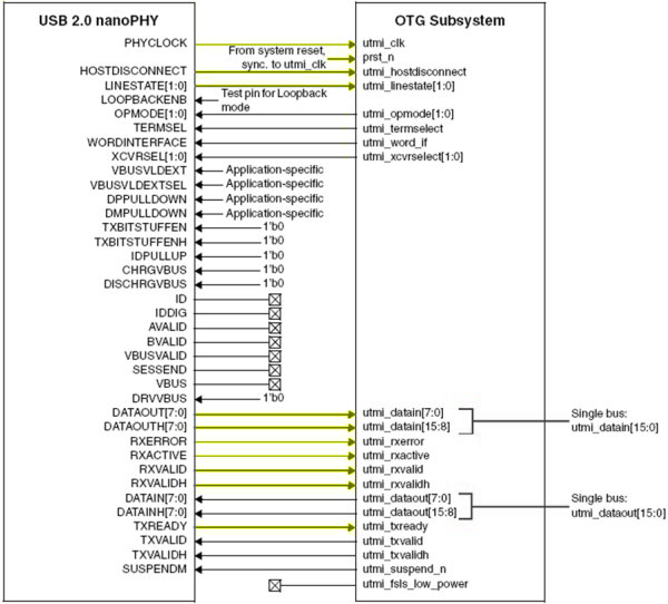
Figure 2. Signal Connections Between the USB 2.0 nanoPHY and USB 2.0 HS OTG Subsystem (Configured to Support the UTMI+ (Level 3, Non-OTG) Specification)
Figure 3 below shows a high-level block diagram of the USB 2.0 nanoPHY and USB 2.0 HS OTG Subsystem when configured to support the UTMI+ (Level, 3, OTG) specification.
Figure 3. USB 2.0 nanoPHY and USB 2.0 HS OTG Subsystem: High-Level Block Diagram
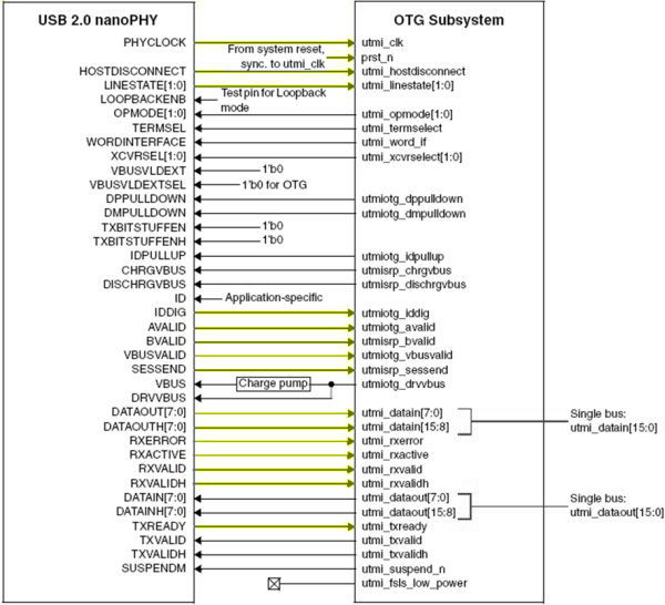
Figure 4. Signal Connections Between the USB 2.0 nanoPHY and USB 2.0 HS OTG Subsystem (Configured to Support the UTMI+ (Level 3, OTG) Specification)
Figure 5 shows the timing for the required power-on reset sequence when the USB 2.0 nanoPHY is attached to the USB 2.0 HS OTG Subsystem. As indicated in Figure 1-1, the USB 2.0 nanoPHY's power-on reset must be released first. When PHYCLOCK is available, the USB 2.0 HS OTG Subsystem's reset can be released. Table 1 describes the timing values for the power-on reset sequence.
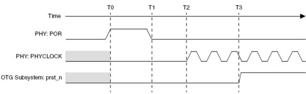
Figure 5. Power-On Reset Sequence for the USB 2.0 nanoPHY and USB 2.0 HS OTG Subsystem
| Timing Parameter | Description | Value |
| T0 | Power-on reset (POR) has been asserted. The USB 2.0 HS OTG Subsystem reset is also asserted. |
0 (reference) |
| T1 | T1 indicates when POR can be released. | T0 + 10μs ≤ T1 |
| T2 | T2 indicates when PHYCLOCK is available at the macro output. | This time depends on the USB 2.0 nanoPHY reference clock source. For information about USB 2.0 nanoPHY power-on reset operation, refer to the USB 2.0 nanoPHY databook. |
| T3 | T3 indicates when the USB 2.0 HS OTG Subsystem reset can be released. | T3 > T2 Note: For information about system clocks and reset in the USB 2.0 HS OTG Subsystem refer to DesignWare Cores USB 2.0 Hi-Speed On-The-Go (OTG) Databook, "System Clocks and Reset" section. |
Search Tools