


Synopsys IP Technical Bulletin Article
PCI Express Switch Enumeration Using VMM-Based DesignWare Verification IP
PCI Express (PCIe) utilizes a point to point interconnect and uses switches to fan out and expand the number of PCIe connections in a system. Upon system boot up a critical task is the discovery or enumeration process of all the devices in the PCIe tree so they can be allocated by the system software. During the enumeration process the system software discovers all of the switch and endpoint devices that are connected to the system, determines the memory requirements and then configures the PCIe devices. The PCIe switch devices represent a special case in this process as their configuration is unique and separate from that of PCIe endpoints. In the simulation testbench environment however, only their configuration is required; the discovery process is not strictly necessary as the number of PCIe devices are known ahead of time. This paper will elucidate the process of switch configuration using Synopsys' PCI Express VMM simulation class libraries for SystemVerilog. First, while the discovery process is not needed within the testbench environment, the testbench must still select the bus numbers and memory address of all the devices. These bus numbers are shown in Figure 1 as Bus#2, Bus#3, Bus#4, and Bus#5. Figure 1 shows the testbench that is used in the remainder of the article.Keith Young, Corporate Applications Engineer
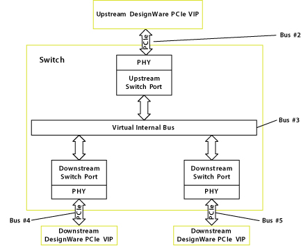
Figure 1. Example Testbench With Bus Numbers Assigned
| Byte Offset | Byte 3 | Byte 2 | Byte 1 | Byte 0 |
|---|---|---|---|---|
| 0x00 | Device ID | Vendor ID | ||
| 0x04 | Status Register | Command Register | ||
| 0x08 | Class Code | Revision ID | ||
| 0x0C | BIST(0x00) | Header Type | Latency Timer | Cache Line Size |
| 0x10 | Base Address Register 0 | |||
| 0x14 | Base Address Register 1 | |||
| 0x18 | Secondary Latency Timer | Subordinate Bus Number | Secondary Bus Number | Primary Bus Number |
| 0x1C | Secondary Status | I/O Limit | I/O Base | |
| 0x20 | Memory Limit | Memory Base | ||
| 0x24 | Prefetchable Memory Limit | Prefetchable Memory Base | ||
| 0x28 | Prefetchable Base Upper 32 Bits | |||
| 0x2C | Prefetchable Limit 32 Upper Bits | |||
| 0x30 | I/O Limit Upper 16 Bits | I/O Base Upper 16 Bits | ||
| 0x34 | Reserved | CapPtr | ||
| 0x38 | Expansion ROM Base Address | |||
| 0x3C | Bridge Control | Interrupt Pin | Interrupt Line | |
| 1. | Command | : Enable memory access |
| 2. | Primary Bus | : Bus number of upstream bus |
| 3. | Secondary Bus | : Bus number of bus directly attached device |
| 4. | Subordinate Bus | : Bus number of farthest downstream device |
| 5. | Memory Limit | : Maximum memory address |
| 6. | Memory Base | : Starting memory address |
| Register | Address | Register | Value |
|---|---|---|---|
| Command[15:0] | 0x04 | 01 | 16'h0004 |
| Primary Bus[7:0] | 0x18 | 06 | 8'b00000010 |
| Secondary Bus[7:0] | 0x18 | 06 | 8'b00000011 |
| Subordinate Bus[7:0] | 0x18 | 06 | 8'b00000110 |
| Memory Base[15:0] | 0x20 | 08 | 16'h0020 |
| Memory Limit[15:0] | 0x20 | 08 | 16'h0060 |
//  Program Upstream Port
//    1)  Write Command register
//    2)  Write Subordinate, Secondary and Primary Bus Numbers
//    3)  Write Memory Limit and Memory Base
task  pcie_rvm_env::Upstream_switch_config();
  begin
      bit test;
      bit status;

      dw_vip_pcie_tlp_transaction  cfg0_wr =
                                   new ( , dw_vip_pcie_tlp_transaction::CFG_WR_0);
      dw_vip_pcie_tlp_transaction  cfg_tlp;

      //  Write COMMAND REGISTER
      //  Enable memory cycles
      test = cfg0_wr.randomize() with {
           m_bvRequesterId == `TBD_REQ_ID;
           m_bvBusNum == 8'h02; m_bvDevNum == 5'h00;
           m_bvFuncNum == 3'h0; m_bvRegNum == 10'h001;
           m_bvFirstDWBE == 4'hF;  m_bTD == 1'b0;
           m_bvvPayload[0] == 32'h00000004;
      };

      if (!test) begin
          `vmm_error(log, "TBD Configuration request packet failed to randomize.");
      end

      $cast(cfg_tlp, cfg_wr.copy());
      tbd_gasket.m_oTlpTxInputChan.put(cfg_tlp);
      cfg_tlp.notify.wait_for(vmm_data::ENDED);
      $cast(cfg_tlp, cfg_wr.copy());
      tbd_gasket.m_oTlpTxInputChan.put(cfg_tlp);

      //  Write Subordinate Bus, Secondary Bus and Primary Bus Numbers:
      test = cfg0_wr.randomize() with {
           m_bvRequesterId == `TBD_REQ_ID;
           m_bvBusNum == 8'h02; m_bvDevNum == 5'h00;
           m_bvFuncNum == 3'h0; m_bvRegNum == 10'h006;
           m_bvFirstDWBE == 4'hF;  m_bTD == 1'b0;
           m_bvvPayload[0] == 32'h00050302;
      };
      if (!test) begin
          `vmm_error(log, "TBD Configuration request packet failed to randomize.");
      end

      cfg_tlp.notify.wait_for(vmm_data::ENDED);

     //  Write Memory Limit and Memory Base
      test = cfg0_wr.randomize() with {
          m_bvRequesterId == `TBD_REQ_ID;
           m_bvBusNum == 8'h02; m_bvDevNum == 5'h00;
	   m_bvFuncNum == 3'h0; m_bvRegNum == 10'h008;
           m_bvFirstDWBE == 4'hF;  m_bTD == 1'b0;
           m_bvvPayload[0] == 32'h00600020;
      };
      if (!test) begin
          `vmm_error(log, "TBD Configuration request packet failed to randomize.");
      end

      $cast(cfg_tlp, cfg_wr.copy());
      tbd_gasket.m_oTlpTxInputChan.put(cfg_tlp);
      cfg_tlp.notify.wait_for(vmm_data::ENDED);
  end
endtask
|
| Register | Address | Register | Value |
|---|---|---|---|
| Command[15:0] | 0x04 | 01 | 16'h0004 |
| Primary Bus[7:0] | 0x18 | 06 | 8'b00000011 |
| Secondary Bus[7:0] | 0x18 | 06 | 8'b00000100 |
| Subordinate Bus[7:0] | 0x18 | 06 | 8'b00000100 |
| Memory Base[15:0] | 0x20 | 08 | 16'h0020 |
| Memory Limit[15:0] | 0x20 | 08 | 16'h0040 |
//  Program Device 1 Downstream Port
//    1)  Write Command register
//    2)  Write Subordinate, Secondary and Primary Bus Numbers
//    3)  Write Memory Limit and Memory Base
task  pcie_rvm_env::Downstream_device_1_switch_config();
  begin
      bit test;

      dw_vip_pcie_tlp_transaction  cfg1_wr =
                                   new ( , dw_vip_pcie_tlp_transaction::CFG_WR_1);
      dw_vip_pcie_tlp_transaction  cfg_tlp;

      //  Write COMMAND REGISTER
      //  Enable memory cycles
      test = cfg1_wr.randomize() with {
           m_bvRequesterId == `TBD_REQ_ID;
           m_bvBusNum == 8'h03; m_bvDevNum == 5'h01;
           m_bvFuncNum == 3'h0; m_bvRegNum == 10'h001;
           m_bvFirstDWBE == 4'hF;  m_bTD == 1'b0;
           m_bvvPayload[0] == 32'h00000004;
      };
      if (!test) begin
          `vmm_error(log, "TBD Configuration request packet failed to randomize.");
      end

      $cast(cfg_tlp, cfg1_wr.copy());
      tbd_gasket.m_oTlpTxInputChan.put(cfg_tlp);
      cfg_tlp.notify.wait_for(vmm_data::ENDED);


      //  Write Subordinate Bus, Secondary Bus and Primary Bus Numbers:
      test = cfg1_wr.randomize() with {
           m_bvRequesterId == `TBD_REQ_ID;
           m_bvBusNum == 8'h03; m_bvDevNum == 5'h01;
           m_bvFuncNum == 3'h0; m_bvRegNum == 10'h006;
           m_bvFirstDWBE == 4'hF;  m_bTD == 1'b0;
           m_bvvPayload[0] == 32'h00040403;
      };
      if (!test) begin
          `vmm_error(log, "TBD Configuration request packet failed to randomize.");
      end

      $cast(cfg_tlp, cfg_wr1.copy());
      tbd_gasket.m_oTlpTxInputChan.put(cfg_tlp);
      cfg_tlp.notify.wait_for(vmm_data::ENDED);

     //  Write Memory Limit and Memory Base
      test = cfg1_wr.randomize() with {
           m_bvRequesterId == `TBD_REQ_ID;
           m_bvBusNum == 8'h03; m_bvDevNum == 5'h01;
           m_bvFuncNum == 3'h0; m_bvRegNum == 10'h008;
           m_bvFirstDWBE == 4'hF;  m_bTD == 1'b0;
           m_bvvPayload[0] == 32'h00400020;
      };
      if (!test) begin
          `vmm_error(log, "TBD Configuration request packet failed to randomize.");
      end

      $cast(cfg_tlp, cfg_wr1.copy());
      tbd_gasket.m_oTlpTxInputChan.put(cfg_tlp);
      cfg_tlp.notify.wait_for(vmm_data::ENDED);


  end
endtask
|
| Register | Address | Register | Value |
|---|---|---|---|
| Command[15:0] | 0x04 | 01 | 16'h0004 |
| Primary Bus[7:0] | 0x18 | 06 | 8'b00000011 |
| Secondary Bus[7:0] | 0x18 | 06 | 8'b00000101 |
| Subordinate Bus[7:0] | 0x18 | 06 | 8'b00000101 |
| Memory Base[15:0] | 0x20 | 08 | 16'h0040 |
| Memory Limit[15:0] | 0x20 | 08 | 16'h0060 |
//  Program Device 2 Downstream Port
//    1)  Write Command register
//    2)  Write Subordinate, Secondary and Primary Bus Numbers
//    3)  Write Memory Limit and Memory Base
task  pcie_rvm_env::Downstream_device_2_switch_config();
  begin
      bit test;

      dw_vip_pcie_tlp_transaction  cfg1_wr =
                                   new ( , dw_vip_pcie_tlp_transaction::CFG_WR_1);
      dw_vip_pcie_tlp_transaction  cfg_tlp;

      //  Write COMMAND REGISTER
      //  Enable memory cycles
      test = cfg1_wr.randomize() with {
           m_bvRequesterId == `TBD_REQ_ID;
           m_bvBusNum == 8'h03; m_bvDevNum == 5'h02;
           m_bvFuncNum == 3'h0; m_bvRegNum == 10'h001;
           m_bvFirstDWBE == 4'hF;  m_bTD == 1'b0;
           m_bvvPayload[0] == 32'h00000004;
      };
      if (!test) begin
          `vmm_error(log, "TBD Configuration request packet failed to randomize.");
      end

      $cast(cfg_tlp, cfg1_wr.copy());
      tbd_gasket.m_oTlpTxInputChan.put(cfg_tlp);
      cfg_tlp.notify.wait_for(vmm_data::ENDED);


      //  Write Subordinate Bus, Secondary Bus and Primary Bus Numbers:
      test = cfg1_wr.randomize() with {
           m_bvRequesterId == `TBD_REQ_ID;
           m_bvBusNum == 8'h03; m_bvDevNum == 5'h02;
           m_bvFuncNum == 3'h0; m_bvRegNum == 10'h006;
           m_bvFirstDWBE == 4'hF;  m_bTD == 1'b0;
           m_bvvPayload[0] == 32'h00050503;
      };
      if (!test) begin
          `vmm_error(log, "TBD Configuration request packet failed to randomize.");
      end

      $cast(cfg_tlp, cfg_wr1.copy());
      tbd_gasket.m_oTlpTxInputChan.put(cfg_tlp);
      cfg_tlp.notify.wait_for(vmm_data::ENDED);

     //  Write Memory Limit and Memory Base
      test = cfg1_wr.randomize() with {
           m_bvRequesterId == `TBD_REQ_ID;
           m_bvBusNum == 8'h03; m_bvDevNum == 5'h01;
           m_bvFuncNum == 3'h0; m_bvRegNum == 10'h008;
           m_bvFirstDWBE == 4'hF;  m_bTD == 1'b0;
           m_bvvPayload[0] == 32'h00600040;
      };
      if (!test) begin
          `vmm_error(log, "TBD Configuration request packet failed to randomize.");
      end

      $cast(cfg_tlp, cfg_wr1.copy());
      tbd_gasket.m_oTlpTxInputChan.put(cfg_tlp);
      cfg_tlp.notify.wait_for(vmm_data::ENDED);

  end
endtask
|
Search Tools