


Synopsys IP Technical Bulletin Article
DDR2/3 SDRAM Controller Options: Protocol or Memory Controller
Access to a large array of cheap, fast, high bandwidth memory is a fundamental requirement of most applications today. Dynamic random access memory (DRAM) has been serving that function for decades, successfully adapting to the market needs over many DRAM generations. DDR2 Synchronous DRAM (SDRAM) has recently succeeded DDR as the highest volume SDRAM, providing higher performance than DDR at a lower cost-per-bit. In the future, DDR3 SDRAM will surpass DDR2 as the highest volume, lowest cost-per-bit SDRAM. One way that SDRAM has continued to keep down per-unit costs has been to keep much of the complexity of accessing and maintaining the SDRAM memory array off the SDRAM die. Instead of placing extra logic on every SDRAM chip, which would drive up the cost of SDRAM, the complex control tasks are made the responsibility of the SDRAM controller. The extra cost, and extra design complexity, is absorbed by a single instance of the SDRAM controller, rather than increasing the logic and cost of every SDRAM chip. Since the industry-driving application for SDRAM is computer systems, and every computer can easily use dozens of SDRAM chips, there is a definitely a computer system cost savings when this design complexity is pushed to the controller. Even though many of today’s SDRAM applications are embedded systems that do not require dozens of SDRAM chips, the controller complexity remains a reality for these alternative applications, as well. This paper will help you define what functionality is required for your next design’s SDRAM controller. It will outline the differences between a full-featured, high bandwidth SDRAM “memory controller” and a lean, efficient SDRAM “protocol controller”, as well as define the benefits of using one or the other in your next design.DDRn Interface Solution
The complete DesignWare DDRn IP solution includes a scalable digital memory controller, an integrated hard macro PHY, and verification IP, as shown here: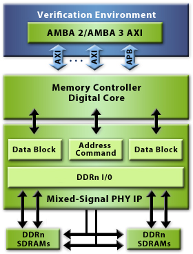
Protocol Complexity, Bandwidth, Latency, and Frequency
The DDRn (DDR, DDR2 or DDR3) SDRAM protocol defines the signal timing requirements for reliable SDRAM usage. The SDRAM controller must continuously monitor the multiple complex timing relationships defined by the DDRn protocol and only issue memory commands and control which comply with the protocol. Any violation of the DDRn protocol can result in memory data corruption. Successful compliance with the DDRn protocol is a minimum requirement for any SDRAM controller. Although DDRn protocol compliance can be challenging, the real challenge of an SDRAM controller is continuously monitoring and complying with the details of the complex protocol while simultaneously achieving high bandwidth and low latency, at an ever-increasing clock frequency. For example, with DDR3 SDRAM each data bit can operate at up to 1600Mbps, using a clock frequency of up to 800MHz. Successfully balancing these multiple design requirements is necessary to create a high performance, reliable, reusable SDRAM controller.Memory Controller and Protocol Controller Defined
For most applications, a flexible, multi-purpose memory controller can be used. The configurable, full-featured DesignWare DDRn SDRAM Memory Controller (MCTL) provides features to support most system requirements. On top of the basic requirement of DDRn protocol compliance, MCTL supports such features as multiple application ports, configurable command and data buffers, programmable arbitration, and memory access reordering to maximize memory bandwidth. Together the MCTL and DesignWare DDRn SDRAM PHY provide a complete memory controller and interface solution, from application masters (such as a CPU or DMA controller) all the way to the chip’s SDRAM I/O, allowing designers to concentrate their efforts on other portions of their chip design. For applications with custom interfaces, special arbitration requirements, or other unique memory access demands not met by a multi-purpose memory controller, the typical solution is to design an application-specific memory controller to interface to the DDRn protocol. The primary value added by application-specific memory controllers is on the application side or scheduling of memory requests, not in the creation of the DDRn protocol commands. Since the DDRn protocol rigidly defines maximum performance for a given series of memory accesses, the DDRn interface can be designed independent of the application-specific portion of the controller with no performance degradation. Using an off-the-shelf protocol controller, like the DesignWare DDRn SDRAM Protocol Controller (PCTL), design engineers responsible for an application-specific memory controller can focus their effort on creating the unique, application-specific front end portion of the controller, such as the custom interfaces and/or specialized scheduler. Once the memory access order is defined by the application-specific front-end, the PCTL provides a simple, easy-to-use native interface (NIF) for memory requests. Design engineers spend their time on the highly differentiating application-specific front end, leaving the off-the-shelf PCTL and DesignWare DDRn SDRAM PHY to handle the well-defined, but complex DDRn protocol and interface. This table provides a summary of the primary features of the PCTL and MCTL:| Controller Function | PCTL | MCTL |
|---|---|---|
| Number of ports to ASIC logic | 1 | Up to 32 |
| Configurable data width conversion (application to/from DDRn) | X | X |
| SDRAM Initialization | X | X |
| Integrated DesignWare PHY calibration and data training | X | X |
| Integrated DesignWare PHY and SDRAM low power control | X | X |
| Optimizes SDRAM precharge/activate command timing | X | X |
| SDRAM refresh control | X | X |
| Arbitration | X | |
| Quality-of-Service (QoS) control | X | |
| Scheduling (memory request re-ordering for higher bandwidth) | X |
Memory Controller (MCTL): Multi-Purpose Memory Access and Scheduling
Most applications require high peak memory bandwidth to satisfy the needs of high bandwidth masters. Many applications support memory requests from multiple unrelated masters, as well. For a wide array of system requirements such as these, the DesignWare MCTL is very well-suited. By providing a wide set of features in an off-the-shelf, configurable component, the MCTL satisfies the performance and system configuration needs of most applications. For systems with multiple masters and/or multiple sub-systems that require access to memory, the MCTL provides up to 32 independent host ports. You may select between multiple arbitration schemes that include both per-command and per-port priorities. Up to eight priority levels are supported providing flexible quality-of-service control across commands and ports. Host port 0 can be programmed to be an ultra-high priority port with reduced latency. A request-acknowledge flow control is used to handle requests from each port. Configurable-depth queues are provided for prioritized commands, scheduled commands and data. The queues provide the ability for the MCTL to prioritize, pipeline, and reorder multiple simultaneous memory requests. Once a memory request has been accepted and prioritized by the MCTL, the physical memory address is internally mapped to the unique bank/row/column addressing required by SDRAM. The MCTL supports automated or fixed address mapping. Software-configurable options provide flexible address mapping, allowing conversion from the physical address to a bank/row/column format, row/bank/column format, or application-specific fixed format. The MCTL’s advanced DDRn command scheduling and reordering techniques improve DDRn data bus utilization by reducing the overhead of bank activation and/or bank precharge. The MCTL bank management and command scheduler keep track of which bank rows (pages) are open so that MCTL can automatically issue bank activate and bank precharge commands. This allows the system masters to issue simple read and write commands without having to worry about scheduling bank activate and bank precharge commands. The MCTL scheduler detects and exploits opportunities to insert bank activate and precharge commands within read/write commands to different banks, reducing the overhead of bank activation and/or precharge. This completes the final translation step from a system master’s read or write command presented at the MCTL host port to the required DDRn protocol-compliant commands which are then issued to the SDRAM through the PHY. Reliable, high-speed DDRn accesses require more than just compliance with the DDRn protocol, but a properly configured and tuned PHY/SDRAM interface. The MCTL includes all the logic required to initialize the DesignWare DDRn SDRAM PHY at power-up and automatically execute data training to ensure reliable data transfers between PHY and SDRAM. From multiple ports and priority control, through address mapping, command scheduling, and DDRn protocol command execution, the feature set available with the DesignWare MCTL will satisfy the memory controller needs of even high performance applications and widely-varying system configurations. The multi-purpose MCTL should be the default option for most applications requiring a DDRn memory controller.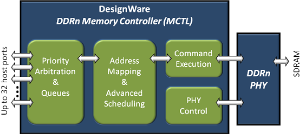
Protocol Controller (PCTL): Efficient Memory Access Translation
For applications that have unique demands that are not met by an off-the-shelf memory controller and instead require application-specific memory control, the DesignWare PCTL is an ideal fit. The low-latency, low-gate count, high bandwidth PCTL handles the details of the DDRn protocol, but does not carry the overhead of the extensive feature set of a standard memory controller. Using the PCTL, a custom-designed, application-specific front end can be isolated from the details of the DDRn protocol. The application-specific front end is able to access memory via simple, synchronous on-chip bus read/write requests to the PCTL. The logic designer is able to focus on the specialized design features necessary to meet the requirements not satisfied by an off-the-shelf memory controller. The PCTL application bus interface supports a lowest-latency “native interface” (NIF). NIF commands use a request-acknowledge two-way flow control. To simplify command processing, the NIF accepts addresses already separated into rank/bank/row/column components. The NIF is burst-based and supports NIF transactions with up to 64 data transfers per NIF read/write command. To maximize data transfer efficiency, NIF data is transferred without flow control, streaming write data from the NIF and read data to the NIF. The PCTL translates NIF memory access requests into highest bandwidth, lowest latency DDRn protocol-compliant commands. NIF bursts are automatically decomposed into the necessary DDRn precharge, activate, read and write commands which are optimally scheduled on the DDRn interface. DDRn precharge and activate commands are bank interleaved to eliminate the bandwidth-reducing overhead of bank activation and precharge whenever possible. The DDRn column commands (reads/writes) strictly follow the order in which the NIF memory access requests were received by the PCTL, providing predictable memory access performance. Application-specific schedulers can benefit from multiple features of the PCTL. For example, both open and close page (row) policies are supported under software control. The PCTL even provides the capability for a NIF transaction to explicitly keep a page open in close page mode. This feature is useful when the custom scheduler generally benefits from using close page mode, but when back-to-back page accesses are detected by the scheduler it can inform the PCTL to keep a bank’s page open and take advantage of the page hit. To enable application-specific scheduler optimization for maximum DDRn data bus bandwidth, PCTL provides continuous feedback on bank “busy” status. Bank busy status allows application-specific schedulers to make informed choices when selecting the next NIF memory access request, based on which banks are currently able to execute new DDRn commands. Similar to the DesignWare MCTL, the PCTL includes all the logic required to initialize the DesignWare DDRn SDRAM PHY at power-up and automatically execute data training to ensure reliable data transfers between PHY and SDRAM. The PCTL provides proven, reliable PHY initialization, training and control. The PCTL offers an easy upgrade path for future designs, since the application-specific front end’s NIF interface can remain the same from one SDRAM generation to the next, such as DDR2 to DDR3. This significantly decreases the uncertainty and risk of upgrading to future SDRAM generations. For systems with specialized interfaces or custom scheduling algorithms necessary to meet memory performance requirements, the DesignWare PCTL combined with DesignWare PHYs can significantly decrease DDRn interface design time and increase design reliability.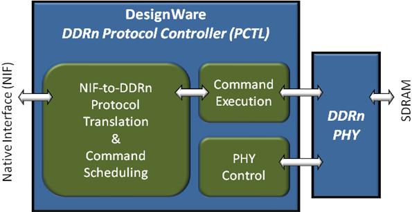
Which is Better for My Design?
The process of servicing memory requests from on-chip masters, such as a CPU, video processor or DMA controller, varies widely depending on your application and system requirements. In general, the more flexible your system requirements, the more likely a multi-purpose memory controller, will meet your design needs. Memory controller IP, like the DesignWare MCTL, is designed to handle a wide variety of system configurations and performance requirements. The MCTL’s multi-port design and flexible prioritization algorithms allow it to be used in most system configurations. The MCTL’s bandwidth-maximizing scheduling algorithms allow it to be used in even very high performance applications. Applications with unique memory access demands may benefit from custom scheduling and arbitration. Similarly, applications with specialized memory requestors often require custom application interfaces. Unique, application-specific features such as these are less likely to be satisfied by standard memory controller IP, however they can definitely benefit from a protocol controller, like the DesignWare PCTL. The PCTL eliminates the need for designers to implement all the complex protocol requirements of DDRn SDRAM, allowing the application to interface to a simple, efficient NIF interface instead. Since the PCTL focuses on just handling the protocol translation and compliance, it easily integrates with application-specific scheduling algorithms or custom interfaces that are sometimes necessary to meet unique system requirements. No matter which controller meets your design needs, the DesignWare MCTL or DesignWare PCTL both seamlessly connect to the DesignWare DDRn SDRAM PHYs. Both the MCTL and PCTL contain the data calibration and data training logic required to properly configure the PHY at system power-up and to ensure reliable data transfers between PHY and SDRAM. Using DesignWare IP for your DDRn SDRAM interface will enable you to spend your engineering time on the other higher value-added features of your system and reliably get your design to market faster.Search Tools