Synopsys IP Technical Bulletin Article

DesignWare DDR3/2 PHY
Requirements for Implementing High Data Rates using Wire-Bond BGA Packaging OverviewThe Synopsys DesignWare® Cores DDR IP portfolio is a complete, silicon-proven, system-level IP interface solution for ASICs, ASSPs, System-on-Chip (SoC) and System-in-Package applications requiring high-performance DDR3/2 SDRAM interfaces operating up to 1600Mbps. The DesignWare DDR3/2 IP is ideal for systems that require the higher performance or lower power consumption of DDR3 while wishing to maintain backward compatibility with DDR2 for maximum design and system cost flexibility. One of the greatest challenges in any SoC that utilizes one or more high speed DDR3 channels (e.g., above the maximum 1066Mbps data rate available with DDR2) is the association that the high speed parallel data channel brings to the packaging technology and PCB design. Wire bond packages are often preferred for their lower cost yet flip chip packaging offers higher performance from a signal integrity perspective due to the lower inductance in the chip connectivity. This paper outlines the impact packaging has on high speed DDR interfaces and presents the requirements that a SoC developer must undertake in order to implement a high speed DDR3 channel with an SoC using wire bond technology. What Makes the DDR SDRAM Interface Sensitive to Package Choice?
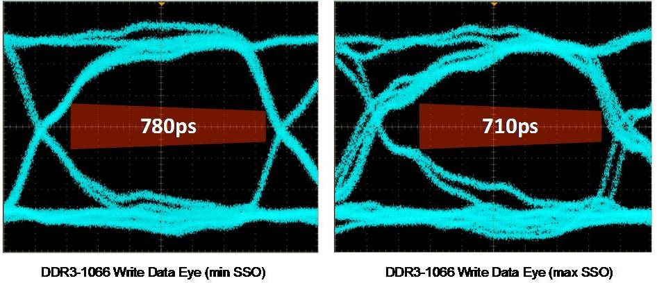
Packaging decisions play a critical role in determining the success or failure of a DDR interface. Poor power delivery characteristics can lead to effects from simultaneously switching outputs (SSO) that slow down the circuitry and distort waveforms leading to timing margin erosion. This effect is highlighted in Figure 1 where the write data eye on the left shows the waveform with a minimum of SSO (only one data bit is switching, the remaining data bits are held at static levels) versus the write data eye on the right that shows all data bits switching concurrently representing the worst case SSO. The data signals shown in all of the data eyes in this paper were measured using the K28.5+ and K28.5- components of the compliance pattern defined for PCI-Express 2.0 that is designed to excite inter-symbol interference and jitter effects. The red trapezoid shown in each data eye presents the data eye width (valid logic levels) expressed in units of time based on clean transitions through VIL / VIH (ac) at the data eye opening and VIH / VIL (dc) at the data eye closing.
 Figure 1: Minimum and Maximum SSO Effect on Data Eye Width in a DDR3 Interface Operating at
1066Mbps - Wire Bond (65nm PHY, 32-bit memory channel, single rank system, typical operating conditions)
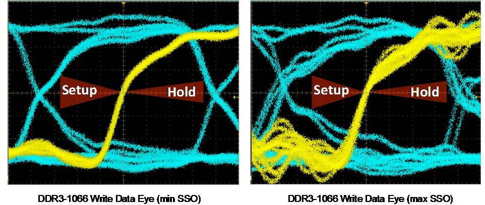
 Figure 2: Minimum and Maximum SSO Effect on Data to Data Strobe Timing in a DDR3 Interface Operating at
1066Mbps - Wire Bond (65nm PHY, 32-bit memory channel, single rank system, typical operating conditions)
- The scenario with minimum SSO achieves ideal setup and hold timing exceeding the DDR3 SDRAM requirements at 1066Mbps
- Worst case SSO shortens the setup time and increases the hold time, effectively shifting the data eye such that the data strobes move out of their optimal location in the data eye
- The noise in the I/O power supplies caused by the maximum SSO case is clearly shown in the yellow data strobe traces as the data transitions.
Electronic packaging serves a distinctly mechanical role. It enables the connections on a fine pitch semiconductor device to be transitioned and attached to wider pitch, easily manufactured printed circuit board. This transition region presents a complex signal and power integrity challenge to the system implementer: distribute clean power to the semiconductor devices while maintaining viable signals being output from and input to the circuit I/Os. The practical reality is that the SoC package is one of the items most often subjected to cost pressures in the semiconductor industry. Most of these pressures concentrate on the power delivery paths in the package. Because of the expense of the silicon, the designer often seeks to reduce the number of pads assigned to power delivery. Concurrently, these same pressures point to using less expensive wire bond technology in lieu of more expensive, lower inductance flip chip. Bond Wire vs. Flip Chip
Flip chip packages have significant signal integrity advantages over wire bond packages. Flip Chip packaging offers lower inductance paths for the power and ground connections, reducing noise on the power rails. There is also less crosstalk in the chip to package substrate connection since tiny bumps replace long wires. Because of the shorter connection, signals also see a more consistent impedance profile in flip chip. The benefit of flip chip for high speed DDR operation is highlighted in Figure 3 which compares to Figure 1 that featured wire bond packaging. However, in Figure 3, the data eyes are shown at 1600Mbps as contrasted to the 1066Mbps data eyes in Figures 1 and 2. Using Synopsys DesignWare Cores DDR3/2 PHY and controller IP as characterized in the same 65nm process used for Figures 1 and 2, notice how the SSO effects in Figure 3 are minimized via the lower power supply inductance, even at the 50% higher data rates as compared to Figure 1. Figure 4 highlights how the lower inductance in the I/O supply rails with the flip chip packaging results in lower supply rail noise and therefore there is less impact on the timing relationship between the data and the data strobes for the maximum SSO scenario as compared to Figure 2.
 Figure 3: Minimum and Maximum SSO Effect on Data Eye Width in a DDR3 Interface Operating at
1600Mbps - Flip Chip (65nm PHY, 32-bit memory channel, single rank system, typical operating conditions)
 Figure 4: Minimum and Maximum SSO Effect on Data to Data Strobe Timing in a DDR3 Interface Operating at
1600Mbps - Flip Chip (65nm PHY, 32-bit memory channel, single rank system, typical operating conditions)
The following are some basic requirements to be considered in the package and PCB designs of systems to support high speed data rates (e.g., DDR3-1333) using a host in wire-bond BGA packaging. This is not meant to be an exhaustive list, nor is it meant to preclude engineering ingenuity; rather it is presented as a list of some of the more important factors to consider. Further guidance for these requirements can be found in the packaging and PCB design application guides provided to licensed users of the Synopsys DDR3/2 SDRAM PHY IP products. Users designing this form of system configuration must be either highly knowledgeable in Signal Integrity analysis, or work with an experienced service provider, such as Synopsys, for Signal Integrity services.
- Maximum 2:1:1 Signal:Power:Ground ratio for SSTL I/O signal (VDDQ) and supply cells (VSSQ) on the die
- Minimum 4-layer package substrate with power and ground planes providing stable signal references
- Short bond wires for I/O power and ground to lower inductance
- VSSQ - less than 1.0mm, 0.7mm maximum recommended
- VDDQ - less than 1.5mm, 1.2mm maximum recommended
- Crosstalk must be minimized in the bond wire region. 3D modeling of the package should be performed to determine the best way to achieve appropriate isolation.
- Maintain low crosstalk between traces. Spacing between etch should be 3X the height of the etch above the reference plane.
- Avoid routing any traces over or near gaps in planes.
- Skew between signals should be kept to a maximum of 5 to 10ps within a byte lane.
- The number of vias connecting a power or ground plane to the balls should equal the number of connections from the package substrate to the power or ground pads on the silicon. This applies to all layers of the substrate.
- Vias should be dispersed about the package to avoid areas of high current concentration.
- Signal vias should be near the reference plane vias. This will minimize the size of current loops reducing crosstalk within the package.
- Make sure package self resonant frequency is not near the desired frequency of operation. The resonant frequency is determined primarily by the on die decoupling and the total inductance of the VDDQ/VSSQ supply loop.

- Build a robust decoupling network that can readily supply current over multiple decades of frequency
- Die, package, and PCB should be modeled extensively. At these frequencies, secondary effects become more important as they consume a larger portion of the timing budget. Modeling the interrelationship between signals and power currents and how they interact with the decoupling network will go a long way to achieving success at higher bit rates.
- Simulate, simulate, and simulate. Spice models should be used in place of IBIS models where possible to increase accuracy.
Synopsys provides a broad portfolio of digital and mixed signal IP cores for system-on-chip designs. As the leading provider of connectivity and analog IP, Synopsys delivers the industry's most complete solutions for widely used protocols such as USB, PCI Express, SATA, Ethernet and DDR/DDR2/DDR3. With high-quality, silicon-proven IP that has been implemented in a wide variety of applications, Synopsys enables designers to accelerate time-to-market and reduce integration risk. For more information on DesignWare IP: www.DesignWare.com